

Pioneer Probe Pins Technology
Co., Ltd.
先鋒探針科技股份有限公司
Discover Our Cutting-Edge AI-Driven Probing Technology


Femto-Second LaserTurning can fabricate complex Micron-sized Probe Pins with ultra-high precision, as well as drill SQUARE(or round) shaped holes for guide plates of Sockets.


With a strong focus on R&D, we leverage advanced materials like Al-SiC, SiC, SiN, and semi-ceramics, and cutting-edge micro-machining processes such as femtosecond lasers, lithography, and electroforming. Our expertise drives the development of next-generation components for GPUs, CPUs, silicon photonics, and medical devices, including human body navigation systems and surgical equipment.
1
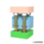
Hi Performance Computing(HPC)
High Speed, High Bandwidth, High Performance , Low Inductance Chip Probing
Large I/O, High Bandwidth, 112G + PAM4
Patented Braided Low profile, with Dia.< 0.3mm & low inductance Probe pin - ideal contacting solution for testing of mobile communications, High speed digital/analog devices(BGA / LGA/QFN) packages with pitches down to 0.35mm)
2
Burn-in & Reliability Tests
Unique One-Body design by press molding ensures ultra-low electrical resistance(below 20 mΩ) with actuation force less than 20 gram/pin.
Dia.< 0.25mm , length < 2.5mm By beryllium copper or Palladium alloy
Patented stamped pins ensures good yield rate, high electrical performance, low test subject damages and less dirt accumulation with lower costs for purchasing.

3
Advanced Conceptual Products
For WLCSP(Wafer Level Chip Scale Packaging)and Emerging AI driven Testing Needs, we can make pogo pin plungers with Dia. smaller than 30µm and fabricate square Probe pins as small as 40µm x 40 µm with Ceramic sockets holes of Aspect Ration greater than 1:20.
Square holes for TGV Interposer of AR> 1:20, Pure-Dry None-Litho CP pins
Guide plate made of PI Film, SiC, Al-AiC, SiN or Engineering Polymer Plastics like PEEK can all be processed by State-of-the-Art Femto-second Laser as well as New Gen. Sub-Micron One-Body Pogo Pins. Precision Parts of Human body Nevacatgion/Treatment system like da Vinci Surgical Machines and Fiber Optic connector Chip modules on of Silicone Photonic Applications

Following ESG trends, we utilize high-precision femtosecond laser with AI positioning instead of water-intensive photolithography. With expertise in CNC, metal stamping, and die-cutting, we provide cost-effective solutions from ICT to semiconductor packaging, including 5-layer metal foil development at 1.76 µm.
Johnny Liu
CEO and Co-Founder of Pioneer

Join Our Team
We’re looking for highly-motivated and talented people to join our innovative team. Submit your application today to join the Pioneer journey!